Just another WordPress site

Just another WordPress site

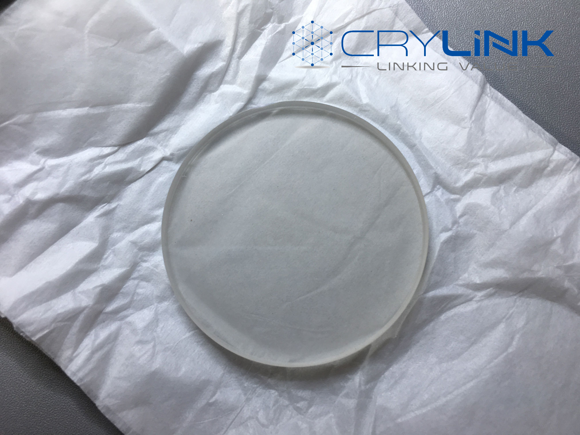
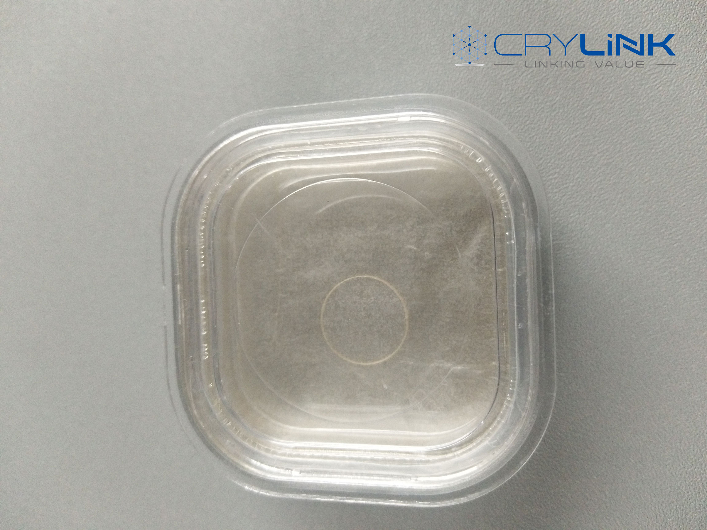
InP’s exceptional electron velocity over silicon and gallium arsenide substrates is used in high-power and high-frequency electronics. InP’s direct bandgap makes it into optoelectronics devices like laser diodes that are used in the optical telecommunications industry, to enable wavelength-division multiplexing.
| Single crystal | Dopant | Conductivity type | Carrier concentration (cm-3) | Mobility (cm2/V·s) | Dislocation density(cm-2) |
| InP | none | N | (0.4-2)×1016 | 3500~4000 | 5×10⁴ |
| InP | S | N | (0.8-3)×1018 (4-6)×1018 | 2000~2400 | 3×10⁴ 2×10³ |
| InP | Zn | P | (0.6-2)×1018 | 1200~3500 | 2×10⁴ |
| InP | Te | N | 107-108 | 2000 | 3×10⁴ 2×10³ |
| Dimension (mm) | Dia 50.8mm x 0.35mm thickness, 10mm x 10mm x 0.35mm | ||||
| Crystal Orientation | -100 | ||||
| Surface roughness | Surface roughness(Ra):<=5A | ||||
| Polishing | Single side polished (SSP) or double side polished (DSP) |


Leave a Reply