InAs Crystal Substrate
Indium arsenide (InAs) is a semiconductor composed of indium and arsenic. It has the appearance of grey cubic crystals with a melting point of 942°C. Indium arsenide is similar to gallium arsenide and is a direct bandgap material. Indium Arsenide wafers are used in mid-infrared Light Emmitting Diods (LEDs) and detectors, and large Hall Coefficient makes a great magnetic field sensor.
InAs single crystal as a substrate can be use to grown InAsSb/In-AsPSb, InNAsSb and other heterojunction materials, Produced wavelength 2~14μm infrared light-emitting devices, InAs single crystal substrate can also be use to epitaxial growth a superlattice structure material AlGaSb, Produce mid-infrared quantum cascade laser. It has good application prospects in the field of gas detection and low loss fiber communication. Besides, the InAs crystal is the ideal material to manufacture the Hall device because of its high electron mobility. Indium arsenide is used for construction of infrared detectors, for the wavelength range of 1–3.8 µm. The detectors are usually photovoltaic photodiodes. Cryogenically cooled detectors have lower noise, but InAs detectors can be used in higher-power applications at room temperature as well. Indium arsenide is also used for making of diode lasers.
Parameter
| Material | InAs | |||
| Growth Method | LEC | |||
| Lattice (A) | a=6.058 | |||
| Structure | M3 | |||
| Melting Point | 942°C | |||
| Density(g/cm3) | 5.66 g/cm3 | |||
| Doped Material | undoped | Sn-doped | S-doped | Zn-doped |
| Type | N | N | N | P |
| Carrier Concentration (cm-3) | 5×10¹⁶ | (5-20)x1017 | (1-10)x1017 | (1-10)x1018 |
| Mobility (cm2v-1s-1) | ≥ 2×10⁴ | 7000-20000 | 6000-20000 | 100-400 |
| EPD (Average) | <5×10⁴/cm2 | <5×10⁴/cm2 | <5×10⁴/cm2 | <5×10⁴/cm2 |
| Size | 2” Dia, 3” Dia, 4” Dia (customized sizes are available) |
| Thickness | 500μm,600μm,800μm(Tolerance:±25μm) |
| Polished | SSP or DSP |
| Orientation | <100>, <111> |
| Redirection Precision | ±0.5° |
| Primary Flat Length | 16±2 mm, 22±2 mm, 32.5±2 mm |
| Scondary Flat Length | 8±1mm,11±1 mm,18±1 mm |
| TTV | <10μm |
| Bow | <10μm |
| Warp | <15μm |
- Direct bandgap material
- A direct bandgap material
- Large Hall Coefficient
- Light emitting diodes
- Laser diodes
- High performance transistors
- Optical application
- Chemical sensing
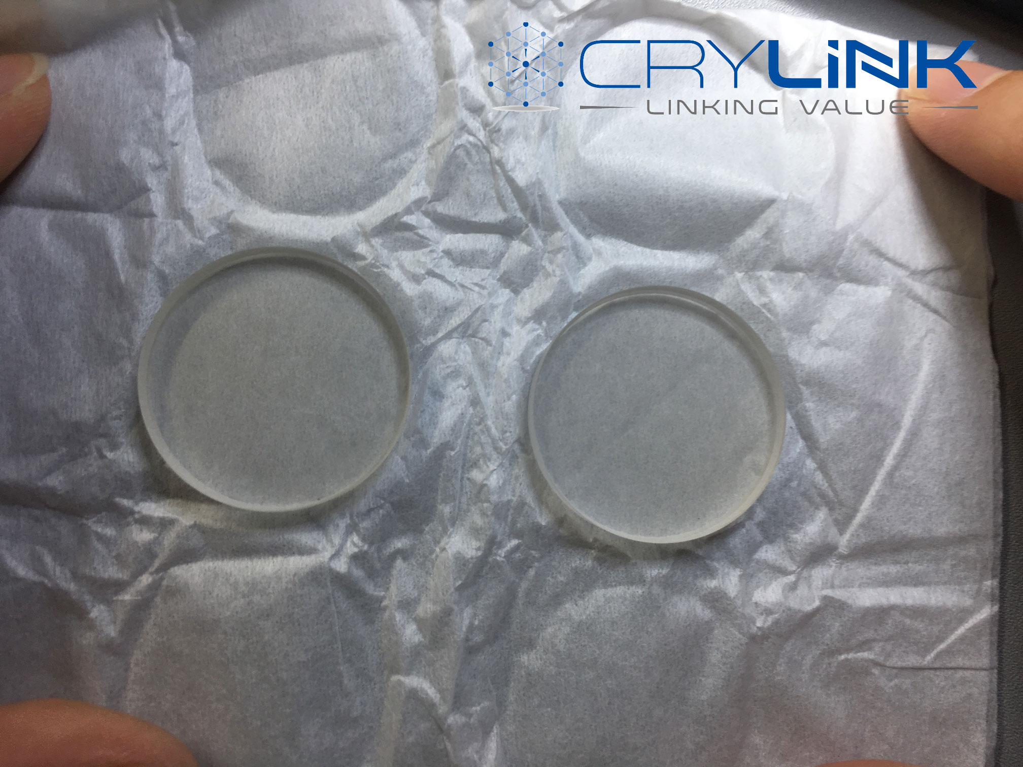
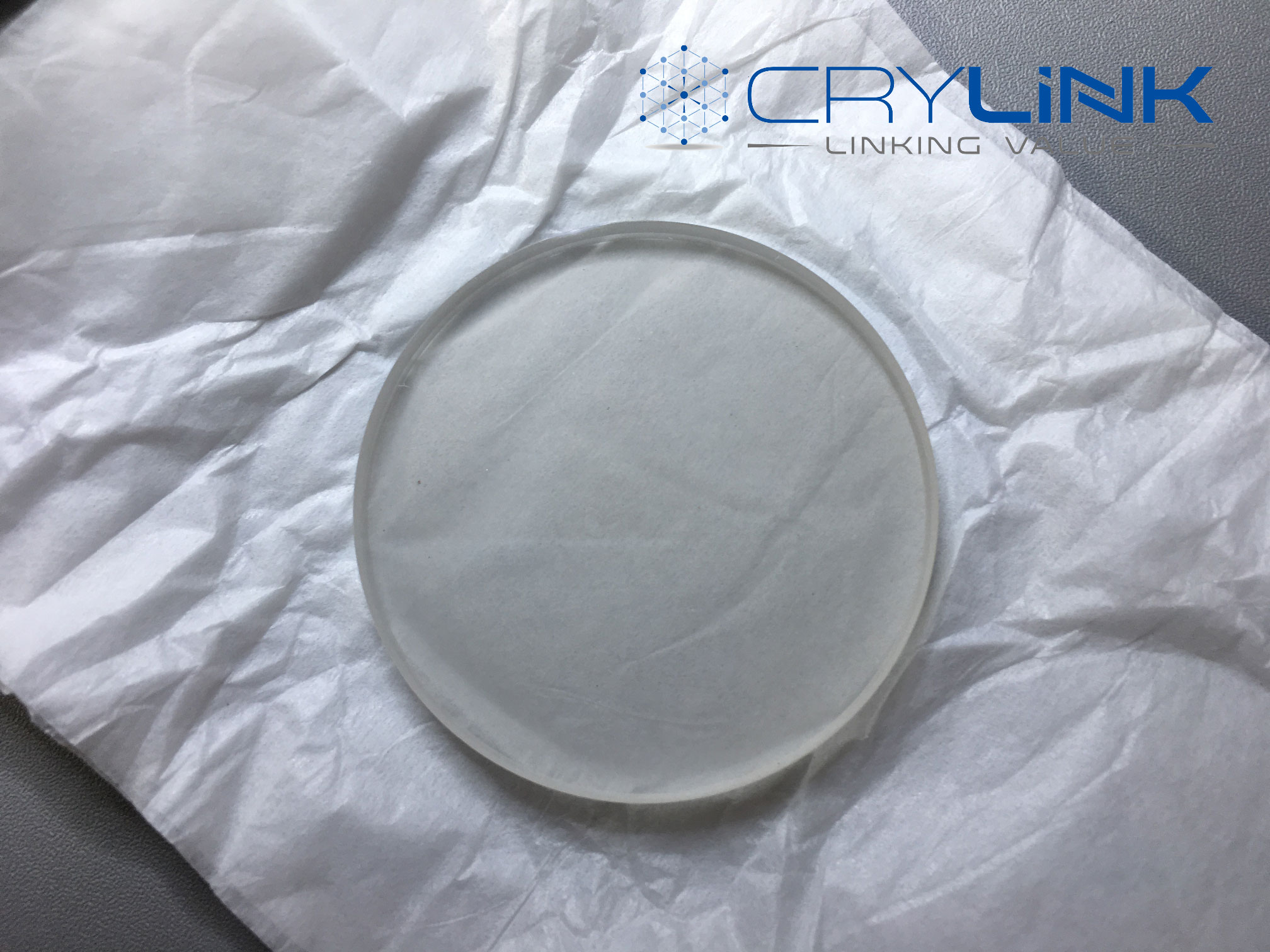
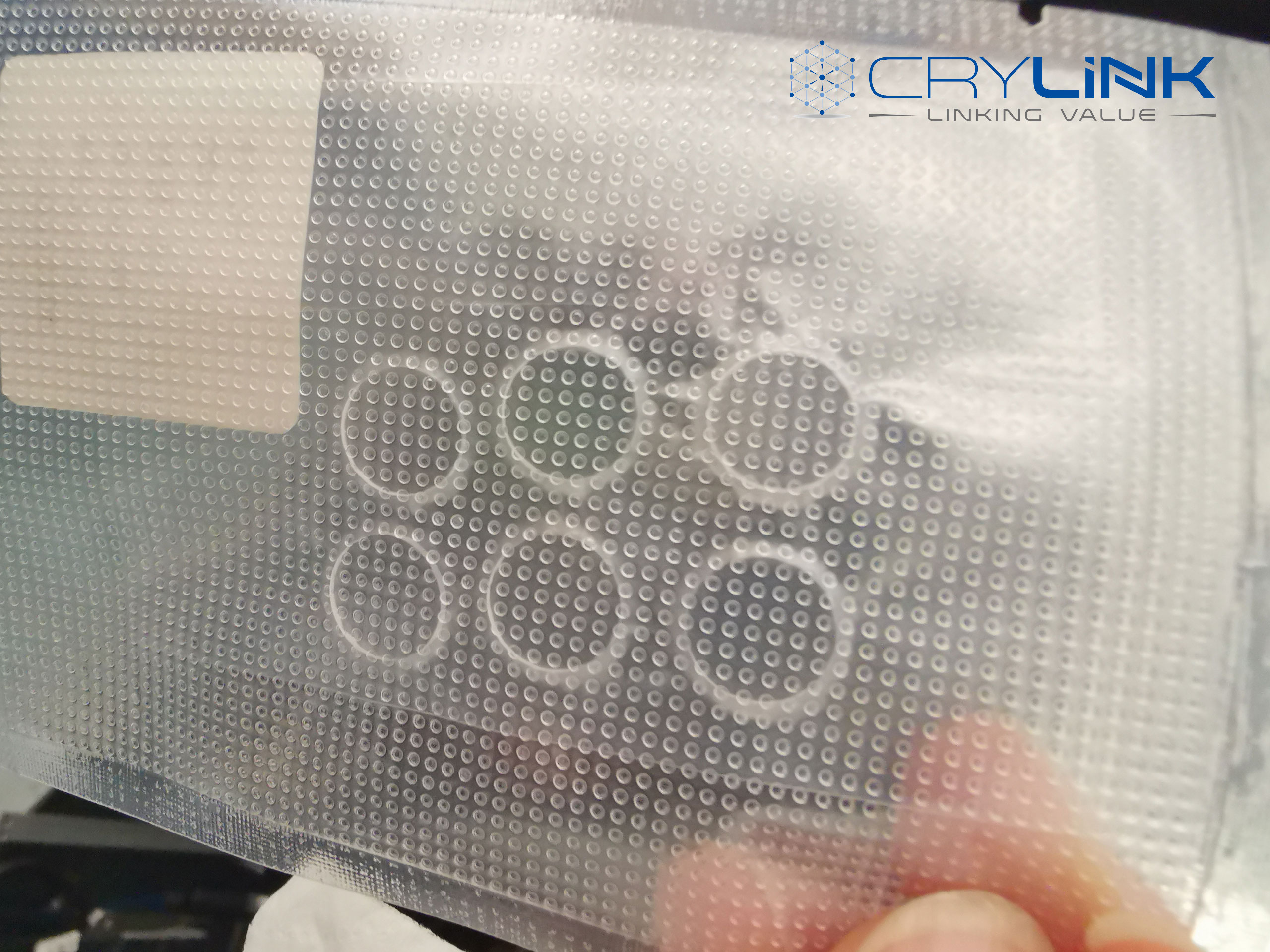
InAs Crystal Substrate have supplied


Leave a Reply