Just another WordPress site

Just another WordPress site

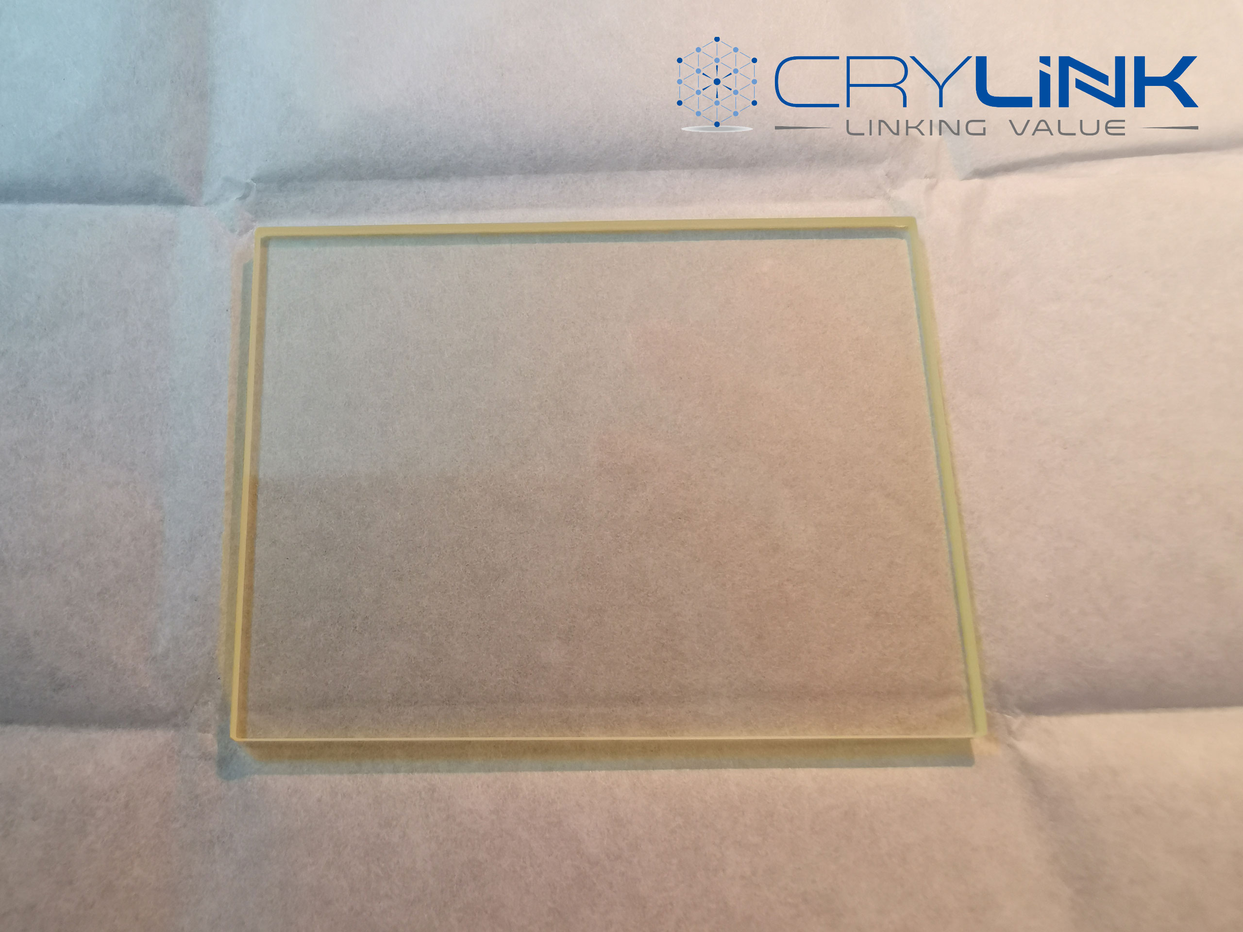
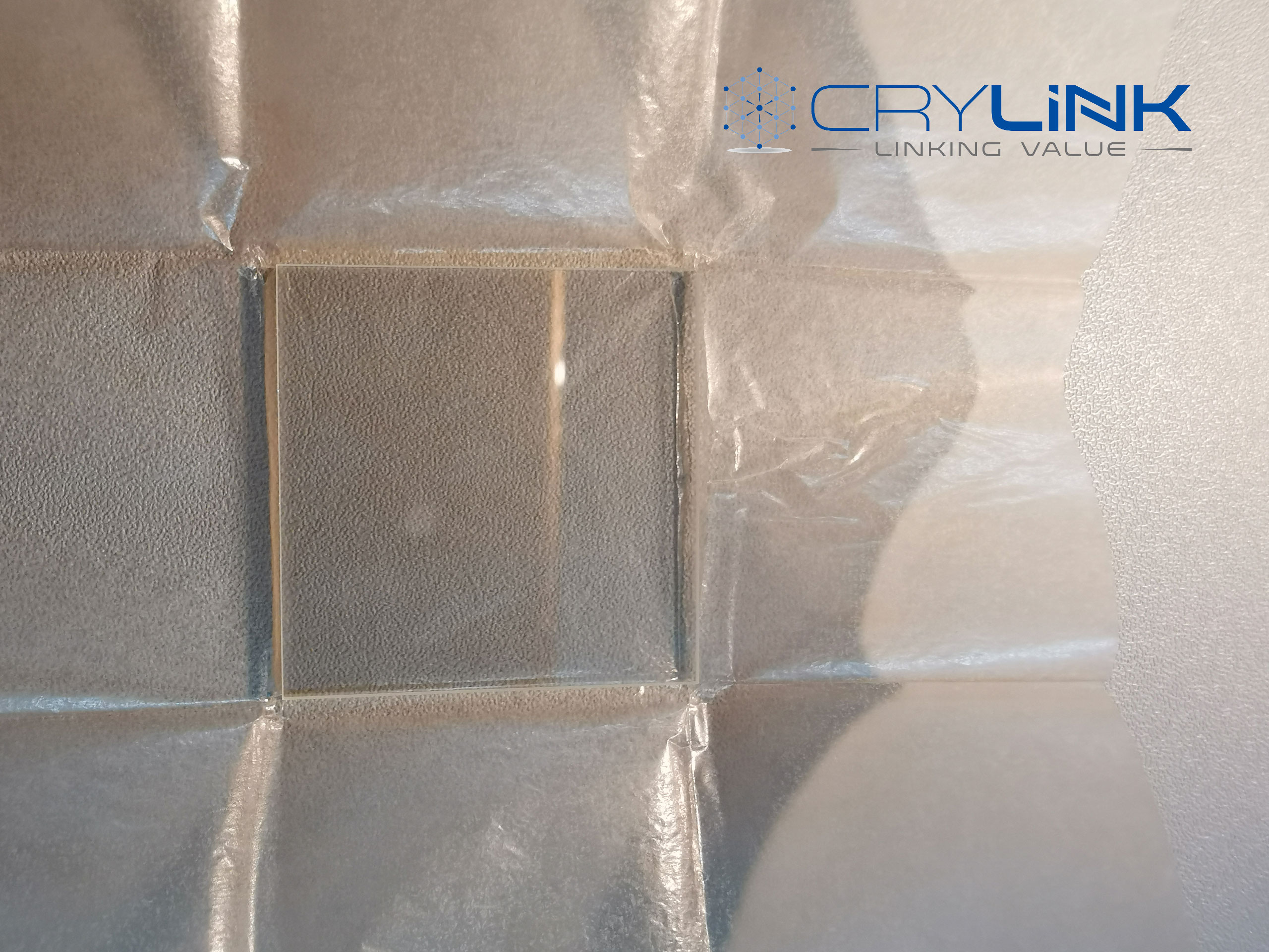
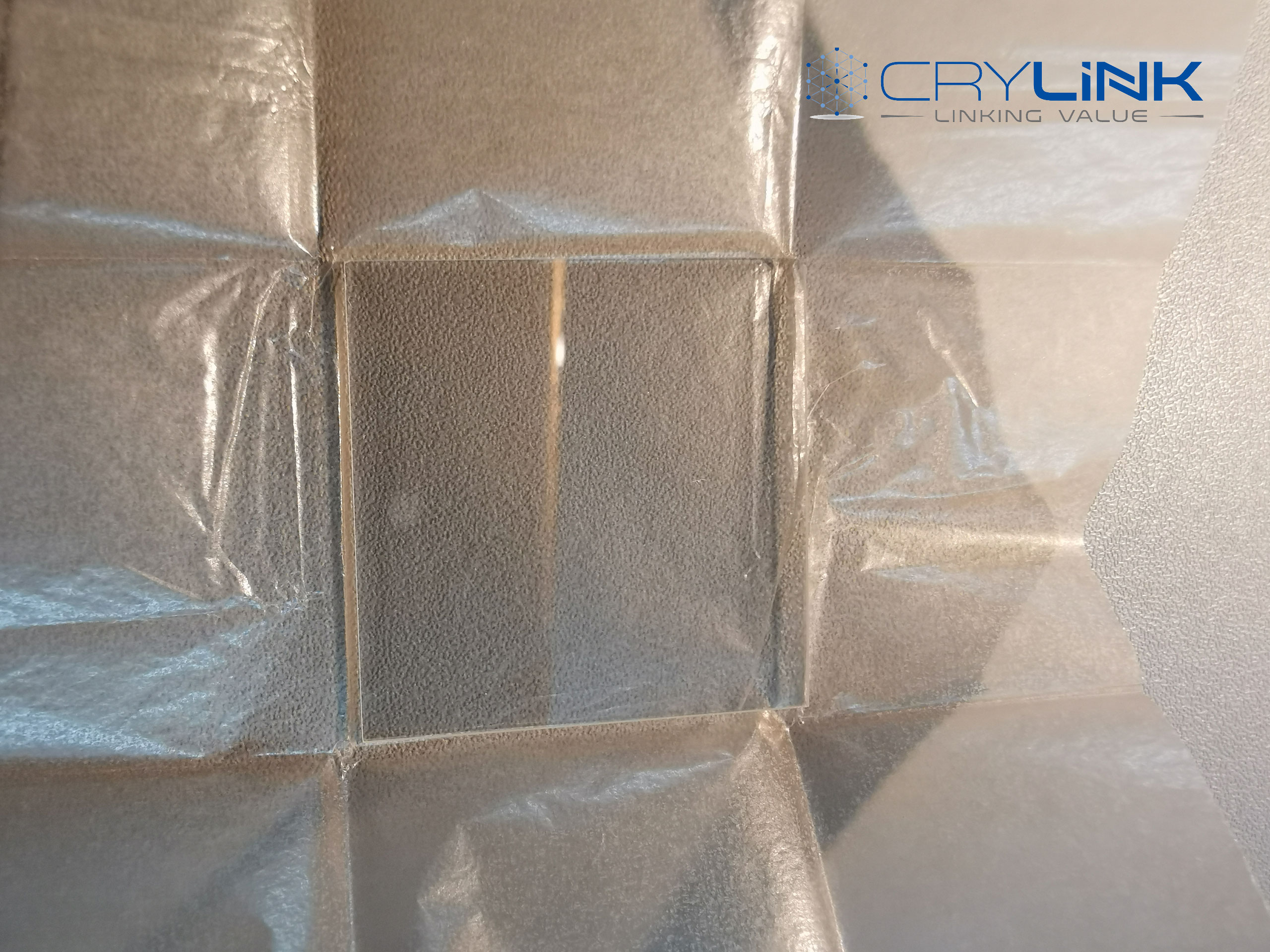
As a rare metal, germanium has many unique properties. Like, Good chemical stability, strong corrosion-resistance, easy processing, high and uniform transmittance, high refractive index, high radiation resistance, high frequency, and good photoelectric performance. The germanium substrates can always be used to manufacture semiconductor devices, infrared optics, and solar cell substrates.
Thanks to the closely-matching thermal and crystallographic properties of germanium and gallium arsenide, epi-ready germanium substrates provide an interesting alternative for the epitaxial growth and/or layer transfer of III-V compounds. For proper nucleation, the wafers are precisely “off-cut” towards the appropriate direction and have been epi-cleaned. Germanium has long been a popular material for integrated circuits. Outside the core area of electronic devices, an EU-funded project is showing its great potential as a substrate to lead next-generation multi-junction solar cells.
| Material | Germanium | ||
| Growth Method | CZ | ||
| Structure | M3 | ||
| Lattice (A) | a=5.65754 | ||
| Melting Point | 937.4°C | ||
| Density(g/cm3) | 5.323 g/cm3 | ||
| Doped Material | undoped | Sb-doped | In/Ga-doped |
| Type | / | N | P |
| Resistivity | >35 Ωcm | 0.05 Ωcm | 0.05~0.1 Ωcm |
| Thermal-expans | <4 x10³/cm2 | <4 x10³/cm2 | <4 x10³/cm2 |
| Size | 10×3, 10×5, 10×10, 15×15, 20x 15, 20x 20,Dia 1”, Dia 2” | |
| Thickness | 0.33mm, 0.43mm 0.5mm, 1.0mm | |
| Polished | SSP or DSP | |
| Orientation | <100>,<110>, <111> | |
| Redirection Precision | ±0.5° | |
| Ra: | ≤5Å(5μm×5μm) | |


Leave a Reply