Just another WordPress site

Just another WordPress site

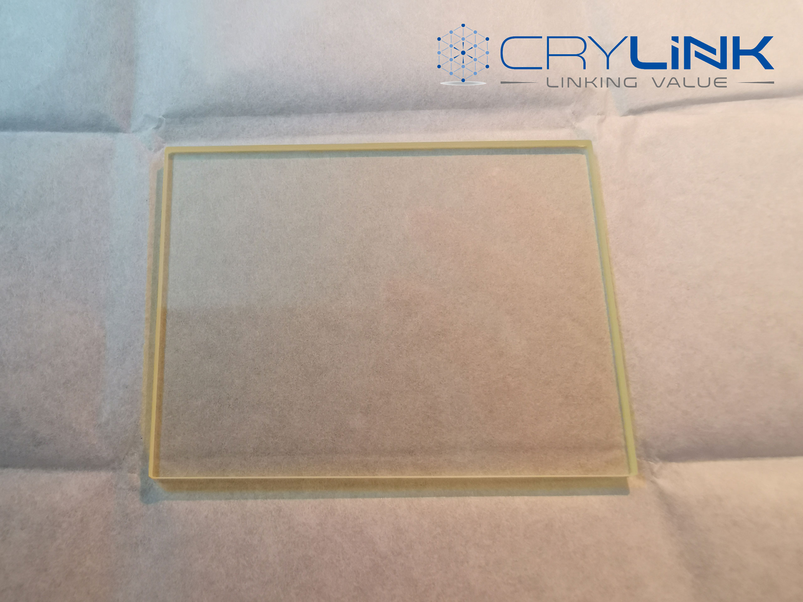
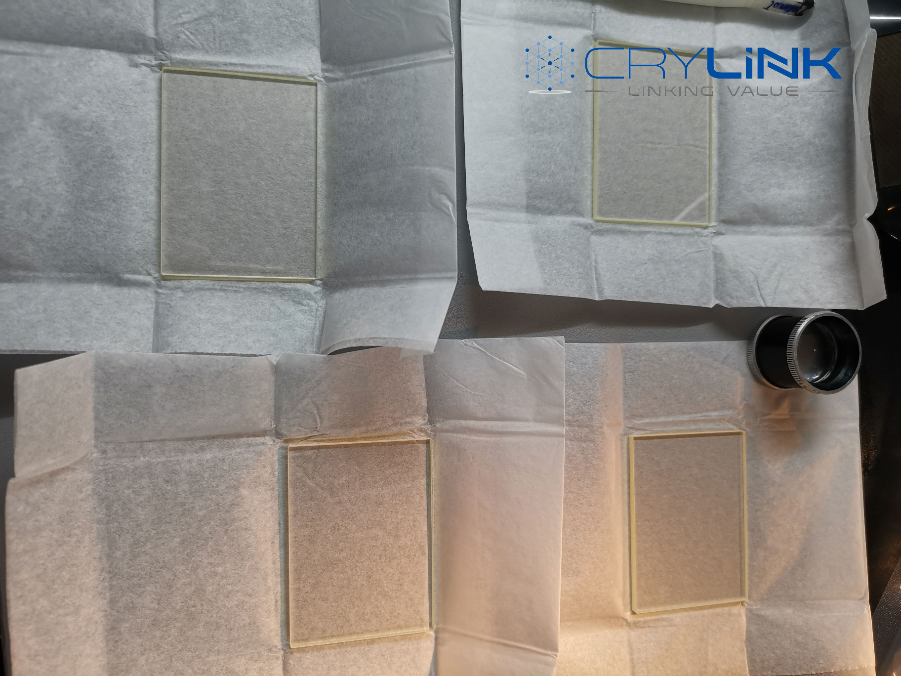
Gallium antimonide (GaSb) is a semiconducting compound of gallium and antimony of the III-V family. It has a lattice constant of about 0.61 nm. GaSb can be used for Infrared detectors, infrared LEDs, infrared lasers and transistors, and thermophotovoltaic systems.
GaSb as a substrate material can be used for the production of certain infrared lasers and detectors of optical fiber transmission. GaSb is also foreseen with a lattice restriction mobility greater than GaAs, so that it has a potential application in the production of microwave devices.
| Single crystal | Dopant | Conductivity type | Carrier concentration (cm-3) | Mobility(cm2/V·s) | Dislocation density(cm-2) |
| GaSb | undoped, intrinsic | P | (1-2)×1017 | 600-700 | <1×10⁴ |
| GaSb | Zn | P | (5-100)×1017 | 200-500 | <1×10⁴ |
| GaSb | Te | N | (1-20)×1017 | 2000-3500 | <1×10⁴ |
| Orientation | <100> / <111> ±0.5° |
| Standard dimension | 20x20x0.5mm, 10x10x0.5mm, 10x5x0.5mm Φ2″x0.5mm, Φ3″x0.6mm,Φ4″x0.8mm Or others upon customer’s requirements |
| Primary Orientation flat Second Orientation flat | 16mm(Φ2″), 22mm(Φ3″), 32.5mm(Φ4″)8mm(Φ2″), 11mm(Φ3″), 16mm(Φ4″) |
| Surface roughness | Ra<=5A (0.5nm) |
| Polishing | Single side Polished or Double side polished |
| TTV / Bow /Warp | TTV <10μm Bow <10μm Warp <15μmTTV <10μm Bow <10μm Warp <15μm |
| Special specification | We can customize specific specification upon requirements |


Leave a Reply