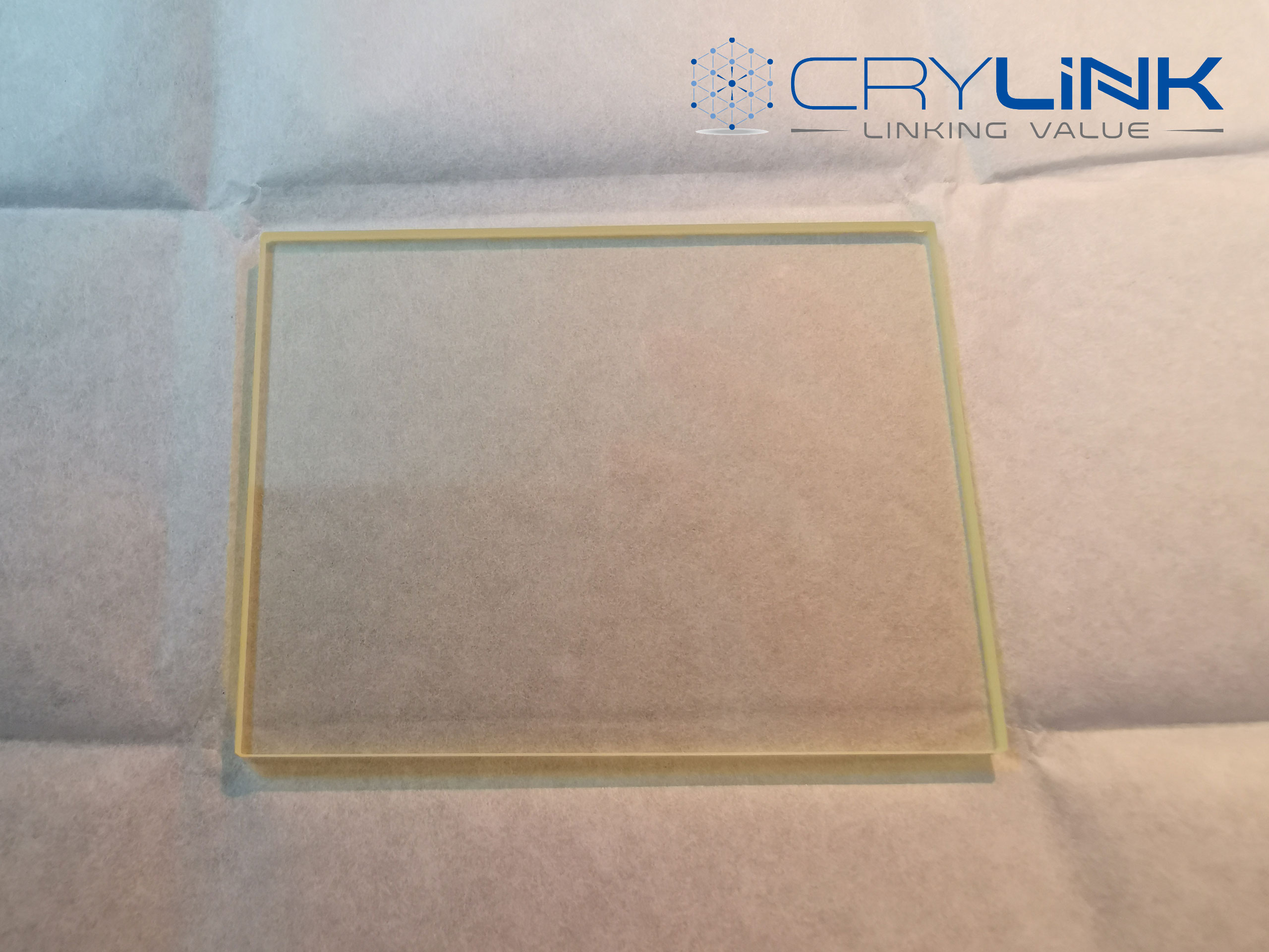
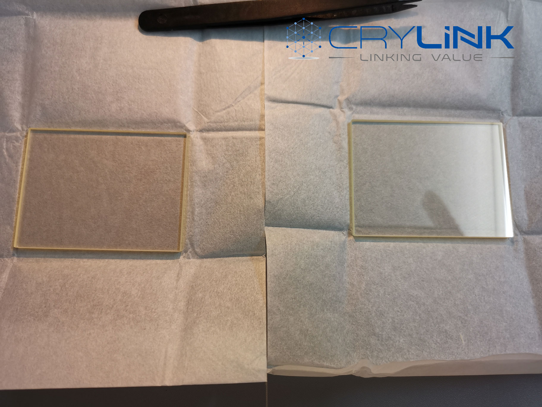
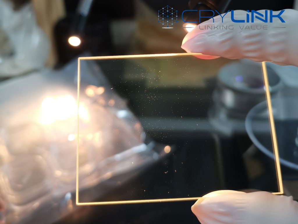
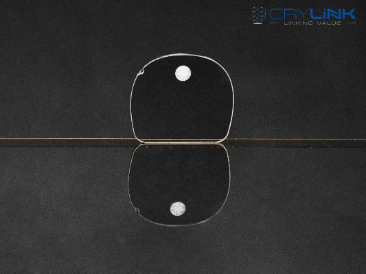
Gallium nitride (GaN) single crystal is a wide-bandgap semiconductor material. Gallium nitrid has broad application prospects in optoelectronic devices, it used as an insulating layer for Ga-based semiconductor materials, and as an ultraviolet filter. It has application prospects in the fields of ultraviolet detectors, gas sensors, light-emitting diodes (LEDs) and. Expecially, Gallium nitride substrates are matched in lattice constant and thermal expansion properties for epitaxial growth of doped GaN layers needed for fabrication of GaN-based devices. This eliminates stress and defects induced by growing GaN epi-layers on non-nitride substrates such as sapphire or silicon carbide, which increase device fabrication complexity and cost and compromise device performance.

Leave a Reply